PRODUCTS
Optical Communication Applicat
-
Active Component Manufacturing
- Optical LD & PD Wafer
- Aspherical Lens and Cap
- TEC Device
- 2.5G-10G APD CHIP
- 10G PIN PD CHIP
- Transimpedance Amplifier
- Aluminum Nitride Substrates
- Alumina substrates
- High Temperature Co-fired Substrates (HTCC)
- 10G CWDM DFB Chip
- Microlens Array
- Smile Corrector
- Slow Axis Collimators(SAC)
- Fast Axis Collimators Arrays(FACA)
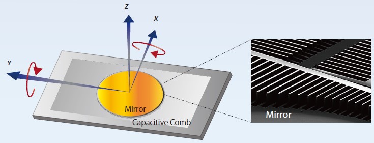
- MEMS Mirror
- SOI Wafers
- Super-thick Thermal Oxidized Wafers
- 25G DFB Laser Diode Chip
-
Test and Measurement
-
High Speed Qptical Transceiver
-
Optical Transport Network Devi
-
Network, Security and Delivery
-
Optical Automation Equipments
-
Passive Component Manufacturin
Industrial Laser and Optical A
-
Lasers
-
Laser Drivers
-
Controller Electronics
-
Optical Components
-
Materials
Solutions
-
BOSA Manufacturing and Packagi
-
ECDL Stable Laser Solution
-
Laser Spectroscopy Solution
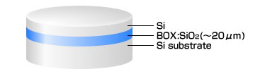
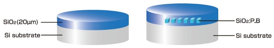
SOI Wafers

SOI(Silicon on Insulator)Wafer is a silicon wafer which is a structured single crystalized layer on oxidized layer and used in the field of high speed LSI, low power LSI, powerdevice, MEMS.
Capability
| Size | 4” 6” 8” |
| Device layer thickness | 100nm※~200μm |
| Wafer in Wafer thickness accuracy | Thin layer ±15nm Thick layer ±0.5μm |
| BOXlayer thickness | Maximum 20μm |
※Thin thickness device layer products is a corroborated products which is manufactured with Shin-Etsu who has a thin device layer making technology and KST’s thick oxidized technology combined together.
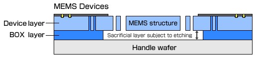
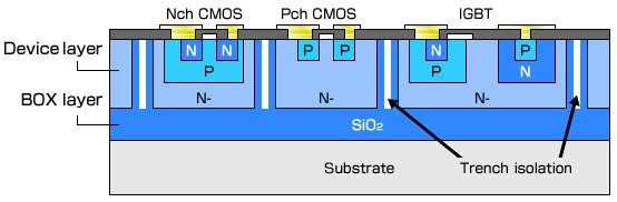
Example of the use of Thick-BOX® SOI Wafer
Supplier

KST service as a wafer foundry providing various services to deposit films on silicon wafers meeting customers’ needs since the establishment of 1998 throughout. Our deposition process service include oxide film, which enjoys the highest demand in the industry today ,and nitride film. In addition, we respond to the diverse needs of customers by creating films of different thickness, from common thin films to thick ones.